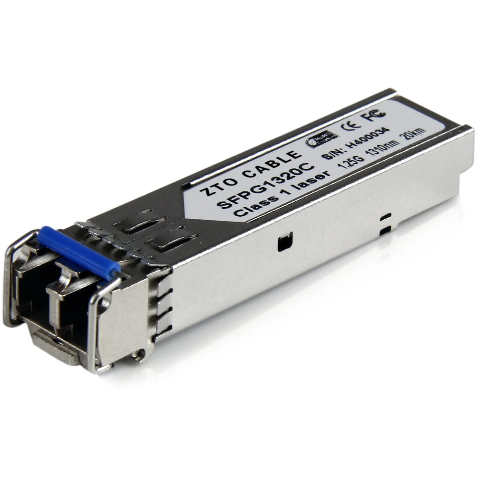
SFP Single Mode DUAL Fiber Transceiver 1.25Gbps 20KM
- Satisfaction guarantee
- Fast delivery
- Quality assurance
Description
Product Features
Uncooled Laser Diode with MQW Structure
InGaAs PIN-TIA Photodiode Receiver
9/125μm SMF
BIDI Single Mode Transceiver SFP Footprint
LC Or SC Optical Interface Are Optional
Compliant With SFP MSA and SFF-8472
Digital Diagnostic Monitoring Interface
Single +3.3V Power Supply
CML Differential Inputs and Outputs
LVTTL Signal Detection Output
Compliant With ITU-T G.957
Compliant With RoHS and Lead Free
Metal Enclosure for Lower EMI Operating Case Temperature:
Standard: 0 to +70°C Extend: -20 to +85°C Industrial: -40 to +85°C
Product Applications
Fast Ethernet
ATM/SONET/SDH Switch/Router
Other Optical Transmission Systems
General Description
The SFP transceivers are high performance, cost effective modules supporting data-rate of 1250 Mbps and 20km transmission distance on 9/125μm SMF.
The transceiver consists of three sections: a laser transmitter, a PIN photodiode integrated with a trans-impedance preamplifier (TIA) and DDMI control unit. All modules satisfy class I laser safety requirements.
The transceivers are compliant with the Small Form-Factor Pluggable (SFP) Multi-Source Agreement (MSA) and SFF-8472. For further information, please refer to SFP MSA.
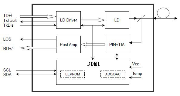
Electrical Specification
| Transmitter | |||||||
| Parameter | Symbol | Min | Typ | Max | Unit | Note | |
| Power Supply Current | ICCT | – | 70 | 150 | mA | 2 | |
| Input Differential Impedance | ZIN | 90 | 100 | 110 | Ω | – | |
| Input Swing Differential Voltage | VIN | 500 | – | 2400 | mV | 3 | |
| TX-Disable Voltage | Disable | – | 2.0 | – | VCC | V | – |
| Enable | – | 0 | – | 0.8 | V | – | |
| TX-Fault Voltage | Fault | – | 2.0 | – | VCC | V | – |
| Normal | – | 0 | – | 0.8 | V | – | |
| Receiver | |||||||
| Parameter | Symbol | Min | Typ | Max | Unit | Note | |
| Power Supply Current | ICCR | – | 70 | 140 | mA | 2 | |
| Output Swing Differential Voltage | VOUT | 600 | – | 2000 | mV | 4 | |
| LOS Voltage | High | – | 2.0 | – | VCC | V | – |
| Low | – | 0 | – | 0.8 | V | – | |
Note: 2. The current excludes the output load current.
3. CML input, internally AC-coupled and terminated.
4. Internally AC-coupled.
Diagnostics Specification
| Parameter | Range | Unit | Accuracy | Calibration |
| Temperature | 0 to +70 | °C | ±3 | Internal/External |
| -40 to +85 | Internal/External | |||
| Voltage | 3.0 to 3.6 | V | ±3% | Internal/External |
| Bias Current | 0 to 100 | mA | ±10% | Internal/External |
| TX Power | -9.5 to -3 | dBm | ±3 | Internal/External |
| RX Power | -22 to -3 | dBm | ±3 | Internal/External |
Pin Definitions
PIN Diagram
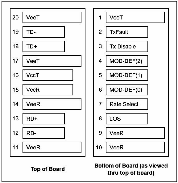
PIN Description
| PIN | Name | Description | Notes |
| 1 | VEET | Transmitter Ground | – |
| 2 | TX FAULT | Transmitter Fault Indication | Note 1 |
| 3 | TX DISABLE | Transmitter Disable | Note 2 |
| 4 | MOD_DEF(2) | SDA Serial Data Signal | Note 3 |
| 5 | MOD_DEF(1) | SCL Serial Clock Signal | Note 3 |
| 6 | MOD_DEF(0) | Module Absent. Grounded within the module | Note 3 |
| 7 | Rate Select | Not Connected | – |
| 8 | LOS | Loss of Signal | Note 4 |
| 9 | VEER | Receiver ground | – |
| 10 | VEER | Receiver ground | – |
| 11 | VEER | Receiver ground | – |
| 12 | RD- | Inv. Received Data Out | Note 5 |
| 13 | RD+ | Received Data Out | Note 5 |
| 14 | VEER | Receiver ground | – |
| 15 | VCCR | Receiver Power Supply | 3.3V±5% |
| 16 | VCCT | Transmitter Power Supply | 3.3V±5% |
| 17 | VEET | Transmitter Ground | – |
| 18 | TD+ | Transmit Data In | Note 6 |
| 19 | TD- | Inv. Transmit Data In | Note 6 |
| 20 | VEET | Transmitter Ground | – |
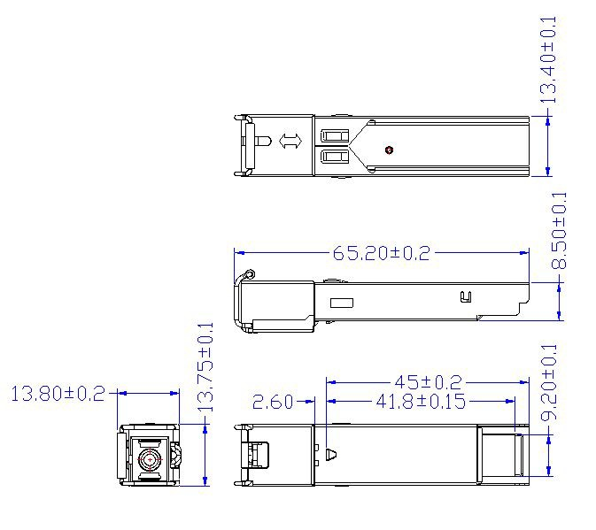
SC Side Interface
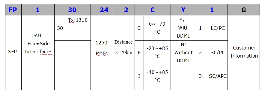
Order Information
